Definitions
- compute-bound - limited by compute cores
- memory-bound - limited by memory bandwidth of the hardware
- resident - how many warps can be parked on an SM as they execute and/or await for memory loads
- issuing warps in SM - how many warps can concurrently issue instructions on any given cycle
- Different arithmetic intensities
- PHY
- memory physical layer - connects memory controller to external memory.
- needed as digital (memory controller) to memory (analog) connection
- Examples
- CPU memory controller (digital) -> PCIe PHY -> analogue waves over PCIe physical infra -> RAM PCIe PHY -> digital signals to RAM memory controller, etc
- GPU memory controller -> HBM PHY -> send analog waves to HBM
- memory physical layer - connects memory controller to external memory.
- DQ (data input, output - D is for data in, Q is for data out)
- individual physical wire within data bus used to transfer raw bits of data back/forth between memory stack and processor
- CA (command address)
- logic die <-(wires consisting of CA and DQ)-> memory dies
- CA bus is unidirectional (memory controller to memory die)
- DQ bus is bidirectional
- thread block cluster - access the memory of any block in the thread block cluster
- local memory
- backed by global memory
- software visibility to threads only
- statically allocated arrays, spilled registers, etc
- Barrier vs Fence
- Execution barrier prevents execution beyond it and synchronize all threads before proceeding
- Memory fence is about ordering
- Interconnect architectures
- Shared bus
- Crossbar
- Tree
- Ring
- Mesh
- Multistage network
- Some mixture
Principles
- matmul square FLOP
- For matrix elements of size
- load matrices, and store a matrix -> of logical memory movement at RAM HBM interface
- note, that memory movement at L2 SM interface and HBM L2 can be different
- latency wise:
- register < local memory (non spilled over) < shared memory < global memory = local memory (spilled over)
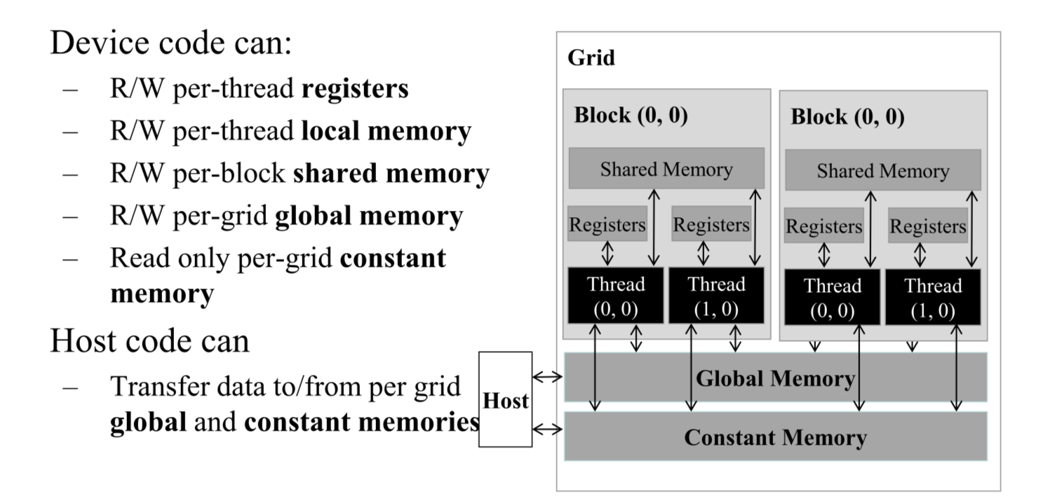
- register < local memory (non spilled over) < shared memory < global memory = local memory (spilled over)
- Tiling moves memory accesses from warp time, loop level, no reuse by other warps in same block to warp time, phase level, reused across warps for same block. The additional memory loads are now done from shared memory which is dramatically faster. The pessimistic amount of data crossing HBM -> on chip memory reduced by a factor of T.
Architecture
Roofline Plot
- X axis can be thought of as how efficient am I w/ each unit of data that I load
- Y axis is "how much more is actually getting done per second"?
- One can see that if one is not very efficient w/ each unit of data load, i.e. load a unit of data then do minimal compute on it then transfer it back, one could imagine that the compute units are sitting idle while the memory loading path is bottlenecked. So the amount of compute done is relatively low.
- Note that there is sort of a bottom bound on how inefficient one could actually be w/ loading data - at worst you do one add or whatever operation per datum loaded, so in reality the roofline plot has a hard cutoff on the x axis at the left - the line will never go to 0.
- Worth noting that inside the memory bound region. is how much bytes we can transfer, is how much compute we can do per byte transferred. We assume here compute is not a bottleneck which is why there is a direct linear relationship between bytes transferred and compute done.
- After a certain amount of data efficiency the compute is the bottleneck. When that is the case the amount of FLOP done per unit time becomes constant because there exists a max throughput of throughput.
HBM data lanes are NOT duplex - i.e.
- The data wires support bidirectional but are buses
- i.e. lower bound for time to transfer data is
- this is different from PCIe (or some other duplex hardware), where lower bound for time to transfer data is
Tiling can very much cause low occupancy due to not enough shared memory if not done with consideration to max supported shared memory per thread.
It is possible to configure CUDA to allow SM to have more shared memory at the expense of other on chip memory resources
Rough memory hierarchy
- HBM stacks (stacked DRAM on package)
- memory controllers and PHYs
- Banked GPU-wide L2 (SRAM, on GPU die)
- on chip fabric/crossbar
- SM owned shared memory
- registers
- SM owned shared memory
- on chip fabric/crossbar
- Banked GPU-wide L2 (SRAM, on GPU die)
- memory controllers and PHYs
- HBM stacks (stacked DRAM on package)
When do we want to turn something into analog?
- Note that PHY is needed for core to core and/or long distance communication because digital signals, afaik, have significant interference (why tho?). The factors at play are
- distance
- synchronous clock domain
- low capacitance and voltage
- in a CPU core (i.e. core asking L1 cache for data) it's purely digital because low distance, synchronous clock domain and low capacitance and voltage.
- Note that PHY is needed for core to core and/or long distance communication because digital signals, afaik, have significant interference (why tho?). The factors at play are
Block admits into SMs are all or nothing - either all warps are resident or none are.
- Without this
__syncthreads()can block for very long periods of time, or possibly even deadlock. Consider a block w/ more threads than the SM has to offer. It will block indefinitely on sync threads.
- Without this
Estimates
Compute done/byte of memory transferred ratio can be estimated as ~GPU flops / GPU max memory bandwidth. Ballpark estimate for kernels' required arithmetic intensity cutoff for compute vs memory bound
Energy consumed from accessing register at least order of mag smaller than DRAM
Syntax
__shared__to put into shared memory- scope w/in thread block
__constant__for constant memory__device__for global (note, if followed by__shared__then it's still thread block)- scope is global
Numbers
- Global memory access ~hundreds of cycles
- H100 ~ 67 TFLOPS (assuming no memory bottleneck which is a bit unrealistic)
- H100 - 64 resident warps per SM, 4 issuing warps per SM per cycle
- H100 ~ 152 B/thread shared memory
Examples
- H100 - 20 FLOP/byte threshold for becoming compute bound
- if you do naive dot product like
for (int k = 0; k < Width; ++k) { Pvalue += M[row * Width + k] * N[k * Width + col]; } - you end up w/ 2 global loads (8 bytes) per 2 flops (1 multiplication, 1 add)
- which is extremely inefficient (0.25 FLOP/byte)
- less than 1% of max throughput of H100!
- if taking into account tensor cores (peak throughput 969 TFLOP/second) - less than 0.01% of the peak!!!
- if you do naive dot product like
Notes
- CUDA blocks always go to one and exactly one SM. A block is never split across multiple SMs
- constant memory gives lower latency reads at the cost of giving up write from GPU side